Ceramic Forum, Glass Manufacturing Technology and Wide-Gap Semiconductors
03-5577-2947
Weekdays: 9:30- 18:00
SiC semi-insulating wafer
セラミックフォーラム株式会社 > Ceramicforum Co., Ltd. > Products > Semiconductor Department > SiC (Silicon Carbide) > SiC semi-insulating wafer
Features of SiC semi-insulating wafers
SiC semi-insulating wafers have wide application for use as a base substrate in high frequency devices (Gallium nitride HEMT). Already in wide use as a transmission amplifier in cellular phone base stations, military radar etc., usage has been steadily increasing over the last few years. In the future, it shows promise for application in automotive radar, large-capacity data transmission etc.
Ceramic Forum began handling SiC semi-insulating wafers in 2011. Semi-insulating SiC wafers are manufactured by high temperature CVD method, which has the following characteristics in comparison with wafers produced by the sublimation method.
・Low rate of defects (low MPD, TSD) -High-resistivity high resistance uniformity in the wafer plane
・High purity

Related Services
Examples of Use
- Transmission amplifier for cellular phone base stations (LTE base stations, Wi-Max base stations, 5G base stations, etc.)
- Military device (radar, missile direction indicator etc.)
- High speed data communication (Broadband broadcasting, satellite data transmission)
- Base substrate for graphene growth
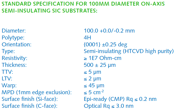
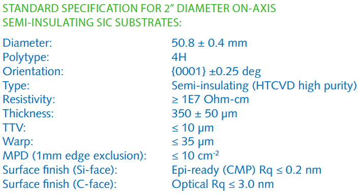
Specifications
For any questions or requests regarding our services please feel free to contact us via phone or inquiry form.
For Telephone Inquiries
03-5577-2947
Weekdays 9:30-18:00
For WEB Inquiries