GaN Wafers
Features of GaN Wafers
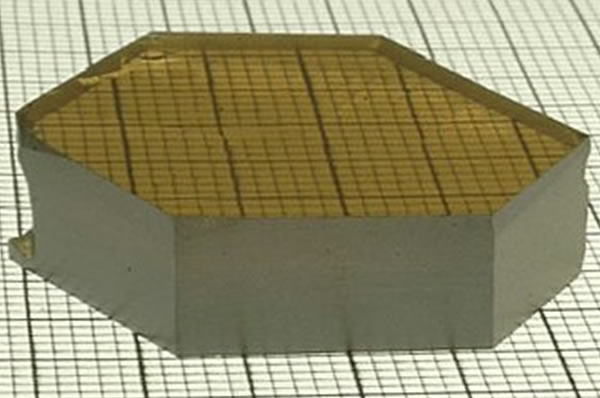
Ceramic Forum began handling GaN wafers manufactured by Ammono (Poland) in 2011.The Ammono GaN substrates are manufactured using the ammonothermal method and boast the world's highest crystalline quality.Especially remarkable is the dislocation density (~ x 10E4) which is lower by two orders of magnitude than other manufacturing methods. Boasting high carrier concentration, it is expected to be adopted for use not only in laser diodes but also in power devices (HEMT transistors, diodes, etc.).
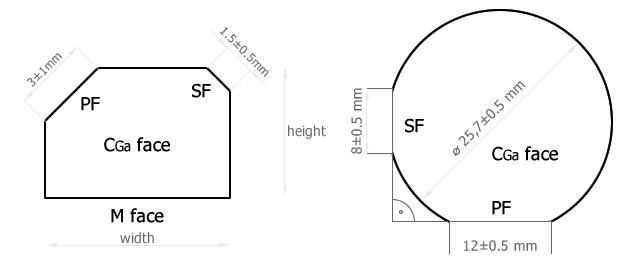
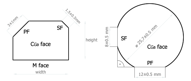
Handling sizes from 10 mm □, to 1 to 2 inches, as well as surface orientation C-plane, non-polar plane, semi-polar plane etc. according to requests.
Future use of GaN semiconductors is likely to grow, and it is expected they will be used in a wide variety of applications.
Currently, Ceramic Forum also handles GaN Wafers manufactured by Nanowin(China). Their GaN substrate is manufactured by HVPE(Hydride Vapor Phase Epitaxy) method. This can be customized according to client's needs. This includes size, thickness, miscut angle, resistivity, doping, polar, and polishing.
Please contact us if interested!

Manufacturer Profile
Ammono (Poland)
Europe's No. 1 free-standing GaN substrate manufacturer.GaN wafers manufactured by this company are rated the highest quality in the world.Based on the Single-crystal GaN R&D project started in 1992 at the University of Warsaw, Poland, Ammono was established in 1999 as a manufacturer specializing in GaN substrate.
As of June 2017, it has a product lineup of m-plane, a-plane and semi-polar plane, as well as c-plane with a maximum aperture of 2 inches.
Examples of Use
- Examples of Use
- Lighting (white LED, UV LED)
- Energy-saving devices (high efficiency, high voltage, high temperature operation devices)
- Storage devices (blue laser diode)
- Radio systems (high frequency devices)
Specifications
High-carrier-concentration n-type GaN substrates
| Features | Units | ORIENTATION | ||
|---|---|---|---|---|
| c-plane | m-plane | 20-21-plane | ||
| Carrier concentration | cm-3 | ~10-19 | ||
| Resistivity | Ω・cm | 10-3ー10-3 | ||
| Mobility | cm2/V・s | ~10-19 | ||
| Thickness | μm | On demand < 1mm | ||
| Total thickness variation(TTV) | μm | < 40 | ~ 20 | ~ 20 |
| Bow | μm | ≦ 10 | ||
| FWHM of X-ray rocking curve,(epi-ready surface at 100 μm × 100μm slit) | arcsec | ~ 20 | ~ 30 | ~ 20 |
| Dislocation density | cm-2 | ~5・104 | ||
| Misorientation | deg | On demand | ||
| Surface finishing | As cut / ground Roughly polished Optically polished (RMS ≦ 3nm) Epi-ready (RMS ≦ 0.5nm) |
|||
| Available sizes | 10 × 10mm 1N |
9 × 13mm 13 × 15mm |
10 × 10mm 13 × 15mm |
|
| Packaging | Separate single wafer container | |||
| Special Order Option | Please, contact Sales Department | |||

High Transparency n-type Gan Substrates Other semi-polar orientation available on request
| Features | Units | ORIENTATION | ||
|---|---|---|---|---|
| c-plane | ||||
| Carrier concentration | cm-3 | ~3・10-17 | ||
| Resistivity | Ω・cm | < 0.5 | ||
| Mobility | cm2/V・s | ~250 | ||
| Thickness | μm | ≥300 | ||
| Total thickness variation(TTV) | μm | ~20 | ||
| Bow | μm | ≤10 | ||
| FWHM of X-ray rocking curve,(epi-ready surface at 100 μm × 100μm slit) | arcsec | ~20 | ||
| Dislocation density | cm-2 | ~5・104 | ||
| Misorientation | deg | On demand | ||
| Surface finishing | As cut / ground Roughly polished Optically polished (RMS < 3nm) Epi-ready (RMS < 0.5nm) |
|||
| Available sizes | 10 × 10mm2, 1N | |||
| Packaging | Separate single wafer container | |||
| Special Order Option | Please, contact Sales Department | |||

Ultra High Resistivity Semi-Insulating GaN substrates
| Features | Units | ORIENTATION | ||
|---|---|---|---|---|
| c-plane | ||||
| Carrier concentration | cm-3 | - | ||
| Resistivity | Ω・cm | 109-1012 | ||
| Mobility | cm2/V・s | - | ||
| Thickness | μm | ≥300 | ||
| Total thickness variation(TTV) | μm | <40 | ||
| Bow | μm | ≤10 | ||
| FWHM of X-ray rocking curve,(epi-ready surface at 100 μm × 100μm slit) | arcsec | ~20 | ||
| Dislocation density | cm-2 | ~5・104 | ||
| Misorientation | deg | On demand | ||
| Surface finishing | As cut / ground Roughly polished Optically polished (RMS < 3nm) Epi-ready (RMS < 0.5nm) |
|||
| Available sizes | 10 × 10mm2, 1.5N | |||
| Packaging | Separate single wafer container | |||
| Special Order Option | Please, contact Sales Department | |||


